Quantcast
Channel: Nerd Ralph
Viewing all 146 articles
Browse latest View live

Powering GPU mining rigs

$
0
0

Since I started mining ethereum almost two years ago, I have found that power distribution is important not just for equipment safety, but also for system stability.  When I started mining I thought my rigs should be fine as long as I used a robust server PSU to power the GPUs, with heavy 16 or 18AWG cables.  After frying one motherboard and more than a couple ATX PSUs, I've learned a lot of careful design and testing is required.

Using Dell, IBM, or HP server power supplies for mining rigs is not a new idea, so I won't go into too much detail about them.  I do recommend making an interlock connector so the server PSU turns on at the same time as the motherboard.  I also recommend only connecting the server PSU to power the GPU PCIe power connectors, as they are isolated from the 12V supply for the motherboard.  If you try to power ribbon risers, the 12V from the ATX and server PSUs will be interconnected and can lead to feedback problems.  Server PSUs are very robust and unlikely to be harmed, but I have killed a cheap 450W ATX PSU this way.  If you use USB risers, they are isolated from the motherboard's 12V supply, and therefore can be safely powered from the server PSU.

In the photo above, you might notice the grounding wire connecting all the cards, which then connects to a server PSU.  I recently added this to the rig after measuring higher current flowing through two of the ground wires connected to the 6-pin PCIe power plugs.  As I mentioned in my post about GPU PCIe power connections, there are only two ground pins, with the third ground wire being connected to the sense pin.  With two ground pins and three power pins, the ground wires carry 50% more current than the 12V wires.  Although the ground wires weren't heating up from the extra current, the connector was.  Adding the ground bypass wire reduced the connector temperature to a reasonable level.

For ATX PSUs, I've used a few of the EVGA 500B, and do not recommend them.  While even my cheap old 300W power supplies use 18AWG wire for the hard drive power connectors, the SATA and molex power cables on the 500B are only 20AWG.  Powering more than one or two risers with a 20AWG cable is a recipe for trouble.  I burned the 12V hard drive power wire on two 500B supplies before I realized this.  I recently purchased a Rosewill 500W 80plus gold PSU that was on sale at Newegg, and it is much better than the EVGA 500B.  The Rosewill uses 18AWG wire in the hard drive cables, and it also has a 12V sense wire in the ATX power connector.  This allows it to compensate for the voltage drop in the cable from the PSU to the motherboard.  The sense wire is the thinner yellow wire in the photo below.

Speaking of voltage drop, I recommend checking the voltage at the PCIe power connector to ensure it is close to 12V.  Most of my cards do not have a back plate, so I can use a multi-meter to measure at the 12V pins of the the power connector where they are soldered to the GPU PCB.  I also recommend checking the temperature of power connectors since good quality low-resistance connectors are just as important as heavy gauge wires.  Warm connectors are OK, but if they so hot that you can't hold your fingers to them, that's a problem.

My last recommendation is for people in North America (and some other places) where 120V AC power is the norm.  Wire up the outlets for your mining rigs for 240 instead of 120.  Power supplies are slightly more efficient at 240V, and will draw half as much current compared to 120V.  Lower current draw means less line loss going to the power supply and therefore less heat generated in power cords and plugs.  Properly designed AC power cables and plugs should never overheat below 10-15 Amps, however I have seen melted and burned connectors at barely over 10A of steady current draw.


Mining with AMDGPU-PRO 17.40 on Linux

$
0
0

A 17.40 beta was released on October 16, with a final release following on October 30th.  There have been some issues with corrupt versions of the final release, but I think they are resolved now.  I encountered lots of problems with this release, which was much of the motivation for making this post.

Until earlier this year, the AMDGPU-PRO drivers were targeted at the new Polaris cards, and support for even relatively recent Tonga was lacking.  Because of this, I was using the fglrx drivers for Tonga and Pitcairn cards.  The primary reason for upgrading now is for large page support, which improves performance on algorithms that use a large amount (2GB or more) of memory.  With the promise of better performance, and since fglrx is no longer being maintained, I decided to upgrade.

I've been using AMDGPU-PRO with kernel 4.10.5 for my Rx 470 cards, so I decided to use the same kernel.  I can't say there is any problems with using a newer kernel like 4.10.17 or even 4.14.5, so they might work just as well.  I left the on-board video enabled (i915), so I would not have to be connecting and disconnecting video cables when testing the GPUs.  After installing Ubuntu 16.04.3, I updated the kernel and rebooted.  For installing the AMDGPU-PRO drivers, I used the px option (amdgpu-pro-install --px), as it is supposed to support mixed iGPU/dGPU use.

My normal procedure for bringing up a multi-GPU machine is to start with a single GPU in the 16x motherboard slot, as this avoids potential issues with flaky risers.  Even with just one R9 380 card in the 16x slot, I was having problems with powerplay.  When it is working, pp_dpm_sclk will show the current clock rate with an asterisk, but this was not happening.  After two days of troubleshooting, I concluded there is a bug with powerplay and some motherboards when using the 16x slot.  When using only the 1x slots, powerplay works fine.

Since I wasn't able to use the 16x motherboard slot, testing card and riser combinations was more difficult.  Normally when I have a problem with a card and riser, I'll move the card to the 16x slot.  If the problems go away, I'll mark the riser as likely defective.  Mining algorithms like ethash use little bandwidth between the CPU and GPU, so there is no performance loss to using 1x risers.  Even the slowest PCIe 1.1 transfer rate is sufficient for mining.  Using "lspci -vv",  I could see the link speed was 5.0GT/s (LnkSta:), which is PCIe gen2 speed.  Reducing the speed to gen1 would mean lower quality risers could be used without encountering errors.

My first thought was to try to set the PCIe speed in the motherboard BIOS.  Setting gen1 in the chipset options made no difference, so perhaps it is only the speed used during boot-up before the OS takes over control of the PCIe bus.  Next, using "modinfo amdgpu", I noticed some module options related to PCIe.  Adding "amdgpu.pcie_gen2=0" had no effect.  Apparently the module no longer supports that option.  I could not find any documentation for the "pcie_gen_cap", but luckily the open-source amdgpu module supports the same module parameter.  By looking at amd_pcie.h in the kernel source code, I determined "0x10001" will limit the link to gen1.  I added "pcie_gen_cap=0x10001" to /etc/default/grub, ran update-grub, and rebooted.  With lspci I was able to see that all the GPUs were running at 2.5GT/s.

For clock control, and monitoring I've previously written about ROC-smi.
====================    ROCm System Management Interface    ====================
================================================================================
 GPU  DID    Temp     AvgPwr   SCLK     MCLK     Fan      Perf    OverDrive  ECC
  3   6938   66.0c    100.172W 858Mhz   1550Mhz  44.71%   manual    0%       N/A
  1   6939   64.0c    112.21W  846Mhz   1550Mhz  42.75%   manual    0%       N/A
  4   6939   62.0c    118.135W 839Mhz   1500Mhz  47.84%   manual    0%       N/A
  2   6939   77.0c    123.78W  839Mhz   1550Mhz  64.71%   manual    0%       N/A
GPU[0]          : PowerPlay not enabled - Cannot get supported clocks
  0   0402   N/A      N/A      N/A      N/A      None%              N/A      N/A
================================================================================
====================           End of ROCm SMI Log          ====================

I also use Kristy's utility to set specific clock rates:
ohgodatool -i 1 --mem-state 3 --mem-clock 1550

Unfortunately ethminer-nr doesn't work with this setup.  I suspect the new driver doesn't support some old OpenCL option, so the fix should be relatively simple, once I make the time to debug it.

Ethereum mining pool comparisons

$
0
0

Since I started mining ethereum, the focus of my optimizations have been on mining software and hardware tuning.  While overclocking and software mining tweaks are the major factor in maximizing earnings, choosing the best mining pool can make a measurable difference as well.

I tested the top three pools with North American servers: Ethermine, Mining Pool Hub, and Nanopool.  I tested mining on each pool, and wrote a small program to monitor pools.  Nanopool came out on the bottom, with Ethermine and Mining Pool Hub both performing well.

I think the biggest difference between pool earnings has to do with latency.  For someone in North America, using a pool in Asia with a network round-trip latency of 200-300ms will result in lower earnings than a North American pool with a network latency of 30-50ms.  The reason is higher latency causes a higher stale share rate.  If it takes 150ms for a share submission to reach the pool, with Ethereum's average block time of 15 seconds, the latency will add 1% to your stale share rate.  How badly that affects your earnings depends on how the pool rewards stale shares, something that is unfortunately not clearly documented on any of the three pools.

When I first started mining I would do simple latency tests using ping.  Following Ethermine's recent migration of their servers to AWS, they no longer respond to ping.  What really matters is not ping response time, but how quickly the pool forwards new jobs and processes submitted shares.  What further an evaluation of different pools, is that they often have multiple servers for one host name.  For example, here are the IP address for us-east1.ethereum.miningpoolhub.com from dig:
us-east1.ethereum.miningpoolhub.com. 32 IN A   192.81.129.199
us-east1.ethereum.miningpoolhub.com. 32 IN A   45.56.112.78
us-east1.ethereum.miningpoolhub.com. 32 IN A   45.33.104.156
us-east1.ethereum.miningpoolhub.com. 32 IN A   45.56.113.50

Even though 45.56.113.50 has a ping time about 40ms lower than 192.81.129.199, the 192.81.129.199 server usually sent new jobs faster than 45.56.113.50.  The difference between the first and last server to send a job was usually 200-300ms.  With nanopool, the difference was much more significant, with the slowest server often sending a new job 2 seconds (2000ms) after the fastest.  Recent updates posted on nanopool's site suggest their servers have been overloaded, such as changing their static difficulty from 5 billion to 10 billion.  Even with miners submitting shares at half the rate, it seems they are still having issues with server loads.

Less than a week ago, us1.ethermine.org resolved to a few different IPs, and now it resolves to a single AWS IP: 18.219.59.155.  I suspect there are at least two different servers using load balancing to respond to requests for the single IP.  By making multiple simultaneous stratum requests and timing the new jobs received, I was able to measure variations of more than 100ms between some jobs.  That seems to confirm my conclusion that there are likely multiple servers with slight variations in their performance.

In order to determine if the timing performance of the pools was actually having an impact on pool earnings, I looked at stats for blocks and uncles mined from etherscan.io.
Those stats show that although Nanopool produces about half as many blocks as Ethermine, it produces more uncles.  Since uncles receive a reward of at most 2.625 ETH vs 3 ETH for a regular block, miners should receive higher payouts on Ethermine than on Nanopool.  Based solely on uncle rate, payouts on Ethermine should be slightly higher than MPH.  Eun, the operator of MPH has been accessible and responsive to questions and suggestions about the pool, while the Ethermine pool operator is not accessible.  As an example of that accessibility, three days ago I emailed MPH about 100% rejects from one of their pool servers.  Thirty-five minutes later I received a response asking me to verify that the issue was resolved after they rebooted the server.

In conclusion, either Ethermine or MPH would make reasonable choices for someone mining in North America.  This pool comparison has also opened my eyes to optimization opportunities in mining software in how pools are chosen.  Until now mining software has done little more than switch pools when a connection is lost or no new jobs are received for a long period of time.  My intention is to have my mining software dynamically switch to mining jobs from the most responsive server instead of requiring an outright failure.

Let's get going!

$
0
0

You might be asking if this is just one more of the many blog posts about go that can be found all over the internet.  I don't want to duplicate what other people have written, so I'll mostly be crypto functions sha3/keccak in go.

Despite a brief experiment with go almost two years ago, I had not done any serious coding in go.  That all changed when early this year I decided to write an ethereum miner from scratch.  After maintaining and improving https://github.com/nerdralph/ethminer-nr, I decided I would like to try something other than C++.  My first attempt was with D, and while it fixes some of the things I dislike about C++, 3rd-party library support is minimal.  After working with it for about a week, I decided to move on.  After some prototyping with python/cython, I settled on go.

After eight years of development, go is quite mature.  As I'll explain later in this blog post, my concerns about code performance were proven to be unwarranted.  Although it is quite mature, I've found it's still new enough that there is room for improvements to be made in go libraries.

Since I'm writing an ethereum miner, I need code that can perform keccak hashing.  Keccak is the same as the official sha-3 standard with a different pad (aka domain separation) byte.  The crypto/sha3 package internally supports the ability to use arbitrary domain separation bytes, but the functionality is not exported.  Therefore I forked the repository and added functions for keccak-256 and keccak-512.  A common operation in crypto is XOR, and the sha3 package includes an optimized XOR implemenation.  This function is not exported either, so I added a fast XOR function as well.

Ethereum's proof-of-work uses a DAG of about 2GB that is generated from a 32MB cache.  This cache and the DAG changes and grows slightly every 30,000 blocks (about 5 days).  Using my modified sha3 library and based on the description from the ethereum wiki, I wrote a test program that connects to a mining pool, gets the current seed hash, and generates the DAG cache.  The final hex string printed out is the last 32 bytes of the cache.  I created an internal debug build of ethminer-nr that also outputs the last 32 bytes of the cache in order to verify that my code works correctly.

When it comes to performance, I had read some old benchmarks that show gcc-go generating much faster code than the stock go compiler (gc).  Things have obviously changed, as the go compiler in my tests was much faster in my tests.  My ETH cache generation test program takes about 3 seconds to run when using the standard go compiler versus 8 seconds with gcc-go using -O3 -march=native.  This is on an Intel G1840 comparing go version go1.9.2 linux/amd64 with go1.6.1 gccgo.  The versions chosen were the latest pre-packaged versions for Ubuntu 16 (golang-1.9 and gccgo-6).  At least for compute-heavy crypto functions, I don't see any point in using gcc-go.


Fast small prime checker in golang

$
0
0
Anyone who does any crypto coding knows that the ability to generate and test prime numbers is important.  A search through the golang crypto packages didn't turn up any function to check if a number is prime.  The "math/big" package has a ProbablyPrime function, but the documentation is unclear on what value of n to use so it is "100% accurate for inputs less than 2⁶⁴".  For the Ethereum miner I am writing, I need a function to check numbers less than 26-bits, so I decided to write my own.

Since int32 is large enough for the biggest number I'll be checking, and 32-bit integer division is usually faster than 64-bit, even on 64-bit platforms, I wrote my prime checking function to take a uint32.  A basic prime checking function will usually test odd divisors up to the square root of N, skipping all even numbers (multiples of two).  My prime checker is slightly more optimized by skipping all multiples of 3.  Here's the code:
func i32Prime(n uint32) bool {
    //    if (n==2)||(n==3) {return true;}
    if n%2 == 0 { return false }
    if n%3 == 0 { return false }
    sqrt := uint32(math.Sqrt(float64(n)))
    for i := uint32(5); i <= sqrt; i += 6 {
        if n%i == 0 { return false }
        if n%(i+2) == 0 { return false }
    }
    return true
}

My code will never call isPrime with small numbers, so I have the first line that checks for two or three commented out.  In order to test and benchmark the function, I wrote prime_test.go.  Run the tests with "go test prime_test.go -bench=. test".  For numbers up to 22 bits, i32Prime is one to two orders of magnitude faster than ProbablyPrime(0).  In absolute terms, on a Celeron G1840 using a single core, BenchmarkPrime reports 998 ns/op.  I considered further optimizing the code to skip multiples of 5, but I don't think the ~20% speed improvement is worth the extra code complexity.


TTL USB dongles: Hacker's duct tape

$
0
0

For micro-controller projects, a TTL serial UART has a multitude of uses.  At a cost that is often under $1, it's not hard to justify having a few of them on hand.  I happen to have several

The first and probably simplest use is a breadboard power supply.  Most USB ports will provide at least 0.5A of 5V power, and the 3.3V regulator built into the UART chip can supply around 250mA.  With a couple of my dongles, I used a pair of pliers to straighten the header pins in order to plug them easily into a breadboard.

I've previously written about how to make an AVR programmer, although now that USBasp clones are widely available for under $2, there is little reason to go through the trouble.  Speaking of the USBasp, they can also be used along with TTL USB dongle to do 2.4Msps 2-channel digital capture.

Since TTL dongles usually have Rx and Tx LEDs, they can be used as simple indicator lights.  To show that a shell script has finished running, just add:
$ cat < /dev/zero > /dev/ttyUSB0
to the end of the script.  The continuous stream of zeros will mean the Tx LED stays brightly illuminated.  To cause the Tx LED to light up or flash for a specific period of time, set the baud rate, then send a specific number of characters:
$ stty -F /dev/ttyUSB0 300
$ echo -n '@@@@@@@@'> /dev/ttyUSB0
Adding a start and a stop bit to 8-bit characters means a total of 10 bits transmitted per characters, so sending 8 characters to the port will take 80 bit-times, which at 300 baud will take 267ms.

It's also possible to generate a clock signal using a UART.  The ASCII code for the letter 'U' is 0x55, which is 01010101 in 8-bit binary.  A UART transmits the least significant bit first, so after adding the start bit (0) and stop bit (1), the output is a continuous stream of alternating ones and zeros.  Simply setting the port to a high baud rate and echoing a stream of Us will generate a clock signal of half the baud rate.  Depending on OS and driver overhead, it may not be possible to pump out a continuous stream of data sending one character at a time from the shell.  Therefore I created a small program in C that will send data in 1KB blocks.  Using this program with a 3mbps baud rate I was able to create a 1.5Mhz clock signal.

If you have server that you remote monitor, you can use TTL dongles to reset a server.  This works best with paired servers, where one server can reset the other.  The RESET pin on a standard PC motherboard works by being pulled to ground, so the wiring is very basic:
RESET <---> TxD
  GND <---> GND
When one server hangs, log into the other, and send a break (extended logic level 0) to the serial port.  That will pull RESET on the hung server low, causing it to reboot.

Debugging debugWire

$
0
0

Many modern AVRs have an on-chip one-wire debugger called debugWire that uses the RESET pin when the DWEN fuse is programmed.  The AVR manuals provide no details on the protocol, and the physical layer description is rather terse: "a wire-AND (open-drain) bi-directional I/O pin with pull-up enabled".  While much of the protocol has been reverse-engineered, my initial experiments with debugWIRE on an ATtiny13 were unreliable.  Suspecting possible issues at the physical layer, I got out my scope to do some measurements.

I started with a single diode as recommended by David Brown.  I used a terminal program to send a break to the AVR, which responds with 0x55 about 150us after the break.  As can be seen in the scope image above, the rise time can be rather slow, especially with Schottky diodes since they have much higher capacitance than standard diodes like a 1N4148.  Instead of a diode, Matti Virkkunen recommends a 1K resistor for debugWIRE.  For UPDI, which looks like an updated version of debugWire, a 4.7K resistor is recommended.  I ended up doing a number of tests with different resistor values, as well as tests with a few transistor-based circuits.  While the best results were with a 2N3904 and a 47K pull-up to Vcc on the base, I achieved quite satisfactory results with a 1.4K resistor:

The Tx low signal from both the Pl2303 and the AVR are slightly below 500mV, which both sides consistently detect as a logic level 0.  With 3.5Vcc, I found that levels above 700mV were not consistently detected as 0.  As can be seen from the scope image, the signal rise time is excellent.  The Tx low from the Pl2303 is slightly lower than the Tx low from the AVR, so a 1.5K resistor would likely be optimal instead of 1.4K.

You might notice in the scope image that there are two zero frames before the 0x55 response from the AVR.  The first is a short break sent to the AVR, and the second is the break that the AVR sends before the 0x55.  While some define a break as a low signal that lasts at least two frame times, the break sent by the AVR is 10 bit-times.  Since debugWire uses 81N, a transmitted zero will be low for 8 bits plus the start bit before going high for the stop bit.  That means the longest valid frame will be low for 9 bit-times, and anything more than 10 bit-times low can be assumed to be a break.  Another thing I discovered was that the AVR does not require a break to enter dW mode after power-up.  A zero frame (low for 9 bit-times) is more than enough to activate dW mode, stopping the execution on the target.  Once in dW mode, a subsequent zero frame will cause the target to continue running, while continuing to wait for additional commands.

My results with a 1.4K resistor are specific to the ATtiny13 + Pl2303 combination I am using.  A different USB-TTL dongle such as a CP2102 or CH340G could have different Tx output impedance, so a different resistor value may be better.  A more universal method would be to use the following basic transistor circuit:

One caveat to be aware of when experimenting with debugWIRE is that depending on your OS and drivers, you may not be able to use custom baud rates.  For example under Windows 7, I could not get my PL2303 adapters to use a custom baud rate.  Under Linux, after confirming from the driver source that custom baud rates are supported, I was eventually able to set the port to the ~71kbps baud rate I needed to communicate with my tiny13.  That adventure is probably worthy of another blog post.  For a sample of what I'll be discussing, you can look at my initial attempt at a utility to detect the dW baud rate of a target AVR.

PiggyFuse HVSP AVR fuse programmer

$
0
0

Although I've been working with AVR MCUs for a number of years now, I had never made a high voltage programmer.  I've seen some HVSP fuse resetter projects I liked, but I don't have a tiny2313.  I think I was also hesitant to hook up 12V to an AVR, since I had fried my first ATMega328 Pro Mini by accidentally connecting a 12V source to VCC.  However, if you want to be an expert AVR hacker, you'll have to tackle high-voltage programming.  Harking back to my Piggy-Prog project, I realized I could do something similar for a fuse resetter, which would simplify the wiring and reduce the parts count.

I considered using a charge pump to provide 12V, like some other HVSP projects do, but adding at least 3 diodes and capacitors would more than double the parts count.  I also realized that most AVR hackers probably have a 12V power source available.  Old ATX power supplies have 12V on the 3.5" floppy connector, which 0.1" pin headers easily plug into.  Old DSL modems and home routers often run from a 12V DC supply.  I decided to use a 14.4V tool battery with a small switching converter.  I even thought of using one of my TL431s, but hooking up a few alligator clips to the switching converter was quicker.

Instead of just copying another program verbatim, I decided to implement the core of the programming algorithm myself.  The AVR datasheets list two algorithms, though all of the HVSP programs I could find followed the first algorithm and not the alternative one.  Both algorithms are somewhat obtuse, and even seem to contradict the datasheet specifications that state the minimum latching time for Prog_enable is only 100ns.

After debugging with my oscilloscope on a tiny13 and a tiny85, I realized that the two parts have different ways of entering HVSP mode.  The tiny13 will enter programming mode when it powers up and finds 12V on the reset pin, while the tiny85 requires the reset pin to be at 0V on power-up before applying 12V.  Although the datasheet doesn't explicitly state it, the target drives SDO high when it has entered HSVP mode and is ready for commands.  In the case of the tiny85, that happens about 300us after applying 12V to the reset pin.  However with the tiny13, that happens much sooner, around 10us.  This means the datasheet's recommendation to hold SDO low for at least 10us 12V has been applied is not only wrong, it's potentially damaging.  During my experimenting, I observed my tiny13 attempting to drive SDO high while the programmer was still holding it low.  That caused VCC to drop from 5V to 4V, likely approaching the 40mA maximum I/O current maximum.  And since the datasheet specifies a minimum VCC of 4.5V for HSVP, the droop to 4V could cause programming errors.  In the scope image, the yellow line is VCC, and the blue line is SDO.

Instead of waiting 300us after applying 12V to send any commands, I considered just waiting for SDO to go high.  While this would work fine for the ATtiny13 and ATtiny85, it's possible some other parts drive SDO high before they are ready to accept commands.  Therefore I decided to stick with the 300us wait.  To avoid the contention on SDO shown in the scope image above, I switch SDO to input immediately after applying 12V.  Since it is grounded up to that point removing any charge on the pin, it's not going to float high once it is switched to input.

Another source of potential problems with other HSVP projects is the size of the resistor on the 12V reset pullup.  I measured as much as 1mA of current through reset pin on a tiny13 when 12V was applied, so using a 1K resistor risks having the voltage drop below the 11.5V minimum required for programming.
I recommend using around 470 Ohms, and use a 12.5V supply if possible.

Putting it all together

As shown in the very first photo, I used a mini-breadboard with the 8-pin ATtiny positioned so that the Pro Mini will plug in with its raw input at the far right.  In the photo I have extra wires connected for debugging.  The only required ones are as follows:
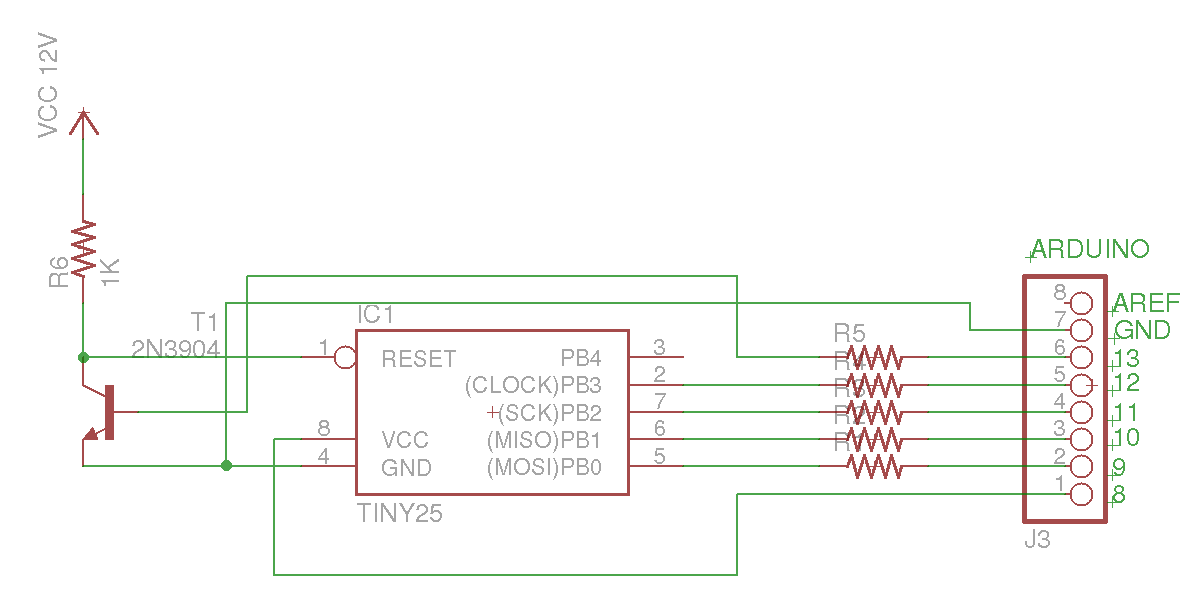
12V supply to RAW on the Pro Mini
GND supply to GND on the Pro Mini
Pullup resistor from 12V supply to ATtiny reset (pin 1)
NPN collector to ATtiny reset
NPN base to Pro Mini pin 11
NPN base to Pro Mini pin 12 & ATtiny GND
ATtiny VCC (pin 8) to Pro Mini pin 6

The Pro Mini must be a 5V version.  The optional resistor from the Pro Mini pin 6 lights the green LED when the Pro Mini has successfully recognized a target ATtiny.  Although the program outputs logs via the serial UART at 57.6kbps, it uses the on-board pin 13 LED to allow for stand-alone operation.  Failure is a long flash for a second followed by 2 seconds off.  Success is one or two short flashes.  One flash is for my preferred debug fuse settings with 1.8V BOD and DWEN along with RSTDISBL.  Two flashes is for my "product" fuse settings with RSTDISBL.  The program will alternate between debug and product fuses each time the Pro Mini is reset.

The code is in my github repo:

And finally, the money shot:


Picoboot Adruino with autobaud

$
0
0

Since the v1 release of picobootSTK500, I've been able to test it on many different Arduino compatible boards.  The biggest problem I've had relates to the various baud rates used by different bootloaders.  Optiboot, which is used on the Uno, uses 115.2kbps, while the Pro Mini m328 uses 57.6kbps.  The default baud rate for the Pro Mini m168 is even lower at 19.2kbps.  While modifying the boards.txt file is not difficult, it introduced unexpected problems.  For testing purposes I keep a couple boards with a stock bootloader, and they won't work unless I change the baud rate back to the default.  I also keep a couple versions of the Arduino IDE for compatibility tests, which adds to the confusion of changing boards.txt files.  Having had some time to think about the best solution, I decided to add automatic baud rate detection to picoboot.

From reading the avrdude source, I knew that it starts communication with the target by sendingthe GET_SYNC command '0' at least 3 times.  '0' is ASCII character 48, and when sent over a serial UART connection, the bitstream including start and stop bits is 0 00001100 1.  With 5 assembler instructions, I can count the low duration of the frame:
1:  sbic UART_PIN, 0 ; wait for start bit
    rjmp 1b
1:  adiw XL, 1 ; count low time
    sbis UART_PIN, 0
    rjmp 1b

The counting loop takes 5 cycles, and since there are 5 low bits, the final counter value is the number of cycles per bit.  Dividing that number by 8 and then subtracting one gives the AVR USART UBRR value in double-speed (U2X) mode.

The Arduino bootloader protocol is almost identical to the stk500 protocol, and so it is relatively easy to write a bootloader that is compatible with both.  For this version I decided to eschew stk500 compatibility in order to save a few bytes of code.  Because of that, and to make it more obvious that it is an Arduino-compatible bootloader, I renamed it to picobootArduino.

With picobootSTK500 v1, a LED on PB5 (Arduino pin 13) was used to indicate that the bootloader was waiting for communication from the host.  In order to make it simpler to use with a bare ATmega168/328 chip on a breadboard, while the bootloader is waiting it brings the Tx pin (PD1) low, which will light up the Rx LED on the connected USB-TTL converter.  As with v1, resetting the AVR will cause it to toggle between the bootloader and the loaded app.  This means it works easily with TTL adapters that do not have a DTR pin for the Arduino auto-reset feature, as well as simplifying it's use with a bare breadboarded AVR.

Despite adding the extra code for the autobaud function, the bootloader is still less than 256 bytes.  In my testing with a 16Mhz Pro Mini clone, the bootloader worked reliably with baud rates from 19,200 to 115,200.  The code and pre-built versions for ATmega328 & ATmega168 are available from my github repo.
https://github.com/nerdralph/picoboot/tree/master/arduino

I also plan to test the bootloader on the mega88 and mega8, where a small bootloader is more beneficial given their limited code size.

Writing small and simple Arduino code

$
0
0

Although Arduino isn't my primary development platform, but I have still used it many times over the past few years.  The intent of Arduino prioritized ease-of-use over efficiency, so when experienced software developers work with it, some degree of holding your nose may be necessary.  Lately I've been making contributions to MicroCore, and therefore the Arduino IDE and libraries.  My most recent impulse buy on Aliexpress is a 7-segment LED & pushbutton module using a TM1638 controller that sells for $1.50, so I decided to test it out using MicroCore.

I found a few existing Arduino libraries for the TM1638, all of which were rather large.  The smallest one I found is TM1638lite, which still uses over half the 1KB flash in a tiny13 for anything more than a minimal use of the library.  At first I considered improving the library, but soon decided the best course would be a full rewrite.

The first problem with the library is a common one since it follows the Arduino library example.  That problem is creating an instance of a class when the use case is that only one instance of the class will be created.  By only supporting a single attached LED&Key module, I can make the library both smaller and simpler.  It also solves another problem common to classes that take pin numbers in their constructor.  It is very easy to mix up the pin numbers.  Take the following example:

TM1638lite tm(4, 7, 8);

Without looking at the library source or documentation, you might think data is pin 4, clock is pin 7 and strobe is pin 8.  Named parameters would solve that problem, but the issue of unnecessarily large code size would remain.  I decided to use a static class in a single header file, which minimizes code size and still maintains type safety.  Writing "const byte TM1638NR::STROBE = 4;" makes it obvious that strobe is pin 4.  With the default Arduino compiler optimization setting, no space is used to sore the STROBE, CLOCK, and DATA variables; they are compiled into the resulting code.

Another improvement I made was related to displaying characters on the 7-segment display.  TM1638lite uses a 128-byte array  to map the segments to light up for a given ASCII character.  Since 7-segment displays can't display characters like "K" and "W", or distinguish "0" from "O", I limited the character set to hex digits 0-9 and "AbCdEF".  The second improvement I made was to store the array in flash (PROGMEM).

I made some additional improvements by code refactoring, and I added the ability to set the display brightness with an optional parameter to the reset() method.  With the final version of the library, the buttons example compiles on the tiny13 to only 270 bytes of code.  You can find the library in my github repo:
https://github.com/nerdralph/nerdralph/tree/master/TM1638NR

Fast 1-wire shift register control

$
0
0

One-wire shift register control systems are an old idea, with the benefit of saving an IO pin at the cost of usually much slower speed than standard SPI.  I'm a bit of a speed nut, so I decided to see how fast I could make a 1-wire shift system.

The maximum speed of 1-wire shift control systems is limited by the charge time of the resistor-capacitor network used.  The well-known RC constant is the resistance in Ohms times the capacitance in Farads, giving the time in seconds to reach 63.2% charge or discharge.  To determine the discharge of a capacitor at an arbitrary time, look at a graph for (1/e)^x:

In a 1-wire shift system, the RC network must discharge less than 50% in order to transmit a 1, and it must discharge more than 50% in order to transmit a 0.  That 50% threshold is 0.7*R*C.  The hysteresis for the shift register and the system error margin will determine how far from 50% those thresholds must be, and therefore the difference between the low times for transmitting a 1 or 0 bit.  The SN74HC595 datasheet indicates a typical margin of about 0.05*Vcc, so an input high must be more than 0.55*Vcc, and input low must be less than 0.45*Vcc.  After writing some prototype code, and a bunch of math, I settled on an order of magnitude difference between the two.  That means in an ideal setup, a transmitted one discharges the RC network by 16.5%, and a zero discharges the network by 83.5%.  That gives a rather comfortable margin of error, and it does not entail significant speed compromises.

Half of the timing considerations in previous 1-wire shift systems is the discharge time, and the other half is the charge time.  That is because after transmitting a bit, the RC network needs to charge back up close to the high value.  In order to eliminate the charge delay, I simply added a diode to the RC network as shown in the schematic.  If you are thinking I forgot the "C" of the RC network, you are mistaken.  Using the knowledge I gained in Parasitic capacitance of AVR MCU pins and Using a 74HC595 as a 74HC164 shift register, I saved a component in my design by using parasitic capacitance in the circuit.

I'm using a silicon diode that has a capacitance of 4pF.  The total capacitance including the 74HC595, the diode, and the resistor on a breadboard is about 13pF.  A permanent circuit with the components soldered on a PCB would likely be around 10pF.  The circuit is designed for AVRs running at 8-16Mhz, so the shortest discharge period for a transmitted zero would be 10 cycles at 16Mhz, or 625ns.  With R*C = 330ns, a 625ns discharge would be 1.9*RC, and the discharge fraction would be 1/e^1.9, or 0.1496.  The discharge time for a transmitted one would be 62.5ns, and the fraction would be 1/e^0.189, or 0.8278.  Considering the diode forward voltage drop keeps the circuit from instantly charging to 100%, the optimal resistor value when running at 16Mhz would be close to 47K Ohm.  In my testing with a tiny13 running at 9.3Mhz on 3.3V, the circuit worked with as little as 12K Ohm and as much as 110K Ohm.  The "sweet spot" was around 36K Ohm, hence my use of 33K in the schematic above.

For debugging with my scope, I needed to count the probe capacitance of ~12pF, which gives a total capacitance of 25pF.  Here's a screen shot using a 22K Ohm resistor, transmitting 0xAA:


I've posted example code on github.  It uses the shiftOne function for software PWM, creating a LED fade effect on all 8 outputs of the shift register.  I tested it with MicroCore, and the shiftOne function can be copied verbatim and used with avr-gcc.  Since it uses direct port access instead of Arduino's slow digitalWrite, the references to PORTB & PINB will need to be changed in order to use a pin on a different port.

Hacking LCD bias networks

$
0
0

Those of you who follow my blog know that I like to tinker with character LCD displays.  Until recently, that tinkering was focused on the software side.  What started me down the road to hacking the hardware was an attempt to reduce the power consumption of the displays.  The photo above shows the modified resistor network used to provide the bias voltages used by the LCD controller.  One end of the resistor ladder is connected to Vcc, and the other is connected to the bias/constrast pin (#3).  My modules came with 5 resistors of 2.2K Ohms each for a total of 11K.  Powered from 5V, the bias network will use about 450uA even when the LCD display is off.  When I changed the middle resistor in the ladder to 15K, the display stopped working, so I started investigating how the voltages are used to drive the LCD.

I remembered coming across an AVR application note on driving LCD displays, which helped explain some of the basic theory.  I also read a Cypress application note on driving LCD displays.  What I lacked was a full description of how the HD44780 drives the LCD, as the manual only describes the waveform for the common lines and not the segment lines.  From the application notes, I knew that the difference between the segment and common lines would be around the LCD threshold voltage.  The first information I found indicated a threshold voltage of over 2V, but modifying the bias resistors for a 2V threshold voltage resulted in a blank display.  Further investigation revealed the threshold voltage to be much lower, close to 1V.  Therefore the segment waveform looks something like the green line in the following diagram:

With the stock 2.2K resistor ladder, my modules gave the best contrast with 0.3-0.4V on the contrast pin.  With Vcc at about 5.05V, that means the difference between each step in the bias ladder was 0.94V.  To confirm the theory, I calculated the resistance values needed to maintain 1.2V between V2 and V3, and ~0.95V between the rest, for a total of 5V.  This means the middle resistor in the ladder needs to be 1.2/0.95 = 1.26 x the resistance of the rest.  Using some 7.5K 0805 resistors I have on hand meant I needed something around 9.5K for the middle resistor.  The next size up I have in chip resistors is 15K, which was too much, but I could re-use one of the original 2.2K resistors in series with a 7.5K to get a close-enough 9.7K.  After the mod, I plugged it into a breadboard, and it worked:

With additional hacking to the bias network, it should even be possible to get the modules to work at 3.3V.  That would require flipping V2 and V3, so that V3 > V2, and V3-V4 = ~1V.  And that likely requires removing the resistor ladder, and adding an external ladder with taps going back to the PCB pads on the LCD module.  That's a project for another day.

A second look at the TM1638 LED & key controller

$
0
0
A few weeks ago I released a small TM1638 library.  My goal was to make the library small and efficient, so I had started with existing libraries which I refactored and optimized.  While looking at the TM1638 datasheet, I thought other libraries might not be following the spec, but since they seemed to work, I followed the same basic framework.  My concern had to do with the clock being inverted from the clock generated by the Arduino shiftOut function.

Figure 8.1 from the datasheet shows the timing for data clocked from the MCU to the TM1638, which the TM1638 samples on the rising edge.  The clock for SPI devices, which shiftOut is intended to control, is low when idle, whereas the TM1638 clock is pulled high when idle with a 10K pull-up. For data that is sent from the TM1638 to the MCU, data is supposed to be sampled after the falling edge of the clock.  After doing some testing at high speed (>16Mhz) that revealed problems reading the buttons pressed, I decided to rewrite the library using open-drain communication, and trying to adhere to the TM1638 specs.

With open-drain communications, the MCU pin is switched to output low (0V) to signal a zero, and switched to input to signal a 1.  When the pin is in input mode, the pull-up resistor on the line brings it high.  The Arduino code to do this is the pinMode function, using OUTPUT to signal low, and INPUT to signal high.  The datasheet specifies a maximum clock rate of 1Mhz, but that appears to be more related to the signal rise time with a 10K pullup than a limit of the speed of it's internal shift registers.  For example I measured a rise time from 0V to 3V of 500ns with my scope:


To account for possibly slower rise times when using longer and therefore higher capacitance wires, before attempting to bring the clock line low, I read it first to ensure it is high.  If is not, the code waits until the line reads high.  As an aside, you may notice from the scope shot, the lines are rather noisy.  I experimented with changing the decoupling capacitors on the board, but it had little effect on the noise.  I also noticed a lot of ringing due to undershoot when the clock, data, or strobe lines are brought low:

I found that adding a series resistor of between 100 and 150 Ohms eliminates the ringing with minimal impact on the fall time.

The updated TM1638 library can be found in my nerdralph github repo:
https://github.com/nerdralph/nerdralph/tree/master/TM1638NR

Using shiftIn with a 74165 shift register

$
0
0

The Arduino shiftIn function is written to be used with a CD4021.  The 74165 shift register is another inexpensive and widely available parallel-input shift register that works slightly different than the 4021.  The logic diagram of the 74HC165 is depicted in the figure above, and shows Qh is connected directly to the output of the 8th flip-flop.  This means that the state of Qh needs to be sampled before the first clock pulse.  With the 4021, the serial output is sampled after the rising edge of the clock.  This can also be determined by looking at the source for shiftIn, which sets the clock pin high before reading the serial data pin:
  for (i = 0; i < 8; i++)  {
    if (bitOrder == LSBFIRST)
      digitalWrite(dataPin, !!(val & (1 << i)));
    else  
      digitalWrite(dataPin, !!(val & (1 << (7 - i))));
      
    digitalWrite(clockPin, HIGH);
    digitalWrite(clockPin, LOW);    
  }

By setting the clock pin high, setting the latch (shift/load) pin high, and then calling shiftIn, the first call to digitalWrite(clockPin, HIGH) will have no effect, since it is already high.  Here's the example code:
  // set CLK high before shiftIn so it works with 74165
  digitalWrite(CLK, HIGH);
  digitalWrite(LATCH, HIGH);
  uint8_t input = shiftIn(DATA, CLK, MSBFIRST);
  digitalWrite(LATCH, LOW);

Like much of the Arduino core, the shiftIn function was not well written.  For a functionally equivalent but faster and smaller version, have a look at MicroCore.

Testing the IBM Cloud

$
0
0

Although I have a Google Cloud free account, I recently decided to try out IBM's Cloud Lite account.  I wasn't just interested in learning, I was also wondering if it could be a viable backup to my Google cloud account.  I'm not concerned with reliability, rather I'm concerned with dependability, since free services could be discontinued or otherwise shutdown.

The Cloud lite description says it includes, "256 MB of instantaneous Cloud Foundry runtime memory, plus 2 GB with Kubernetes Clusters".  I hadn't heard of Kubernetes before, but from a quick review of their web site, it appears to be a platform for deploying scalable docker images. For comparison, the Google compute platform which provides a Linux (Ubuntu 16.04 in my case) VM with 512MB of RAM and 30GB of disk.  I prefer the simplicity and familiarity of a Linux VM with full root access, but I thought there still should be a way to run a LAMP image with Kubernetes.

The IBM Cloud dashboard allows you to choose from the available services based on your account options.  Choosing the IBM Cloud Kubernetes Service from the dashboard links to another page to create a cluster.  However clicking on the create cluster button brings up a new page with the message: "Kubernetes clusters are not available with your current account type."  I opened up a support ticket about it, but after 10 days there has been no action on the ticket.

Since the Kubernetes wasn't working, I decided to try Cloud Foundry Apps.  In order to use cloud foundry, it is necessary to download their commandline tools.  With the Google cloud you get access to a development shell separate from your compute instance VM, and that shell has all the google cloud tools pre-installed.  This is one way the Google cloud is easier and simpler to use.

Instead of setting up a bare cloud foundry app, I decided to use their boilerplate Flask application.  The setup process in the web dashboard lets you choose a subdomain of mybluemix.net, so I chose http://rd-flask.mybluemix.net/.  In order to modify the app, IBM's docs instruct you to download the sample code, make changes locally, then push the changes to the could using their CLI tools.  However, at least in the case of the Python Flask app, there was no download instructions, and no link to the sample code.  After going through the CLI docs, I found it is possible to ssh into the vm instance for your app using "bluemix cf ssh". Yet any changes I made to the code online were wiped whenever I restarted the service.

After some more research, I realized this problem is several months old. In the end, I was able to find an earlier version of the template code, fork it, and updated it to match the code running in the app container. The repo I forked specified "python-2.7.11" in runtime.txt, but the cloud foundry only supports 2.7.12 & 2.7.13 (along 3.x). At first I changed it to 2.7.12 in my fork, but then I removed the runtime.txt so it will use the default version of python. I also added some brief instructions on uploading it to the IBM cloud. You'll find the fork at https://github.com/nerdralph/Flask-Demo.


Sonoff S26: OK hardware, bad app

$
0
0
After I read about the Sonoff S26, and that it is compatible with Google home, I decided to order a couple of them.  In addition to using them as a remote-controlled power switch, I'm interested in resuming my experimentation with the esp8266 that the devices use.

The physical construction is OK, though, as can be seen from the photo above, the logo is upside-down.  I know there is some debate over which way a Nema 5-15R outlet should be oriented, with the ground down being more common in residential, and ground up perhaps being more common in commercial.  The readability of the logo does not effect functionality, so that's not a big deal.  What does effect functionality is the size of the S26, which can partially block the ability to use both outlets.

Cnx-software has a teardown of the S26, so I won't bother repeating any of the details.  The unit I received was virtually indistinguishable from the one depicted in the teardown.  The one slight difference I noticed was the esp8266 module in my S26 has a hot air solder leveling finish (HASL) instead of electroless nickel immersion gold (ENIG).

The eWeLink app is my biggest gripe about the s26.  In order to install the app, it requires numerous permissions that have nothing to do with controlling the s26.  Things like access to device location and contacts are an invasion of privacy, and a liability for itead if someone hacks their database and gets access to all the personal information from eWeLink users.  The only permission the app should need is local wifi network access.

After holding my nose over the permission requirements, it didn't get much better once the app was installed.  It does not work in landscape mode, and once you create an account, it doesn't remember the email when it gets you to log in to the newly created account.  The menus and some of the fonts are rather small, especially on an older phone with a 4" screen.

I also tested out the firmware update function in the app.  My s26 came with v1.6 firmware, which I updated to v1.8.  The new firmware version is supposed to support direct device control over the LAN without an active internet connection.  After the upgrade the device info indicated it was running the new firmware, but direct LAN control did not work.  Without an active internet connection, when I tried turning the s26 on, I got an "operation failed" message.

My last gripe is about the cumbersome process of setting up devices to work with Google home devices.  Having to first setup an account for the Sonoff devices, then having to link that account with the google home account is cumbersome and error-prone.  The google home app should be able to scan for devices the same way it can scan the local network and find a Chromecast.  And for people that are using Sonoff devices without Google home or Amazon, the app should allow users to control devices locally without having to set up any account.

Reading extended signature bytes with AVRdude

$
0
0

AVR MCUs like the ATtiny85 and the ATtiny13 store their signature and RC oscillator data in a special page of flash.  Just like the flash for program storage, this special page of flash can be erased and reprogrammed.  If you are not careful with your ICSP connections, it's not hard to accidentally erase this special page of flash.  I have 2 ATtiny13 chips that had their signature erased when I forgot to connect the power wire from a USBasp.  The voltage on the MOSI and SCK lines was enough to power up the ATtiny13, but without a stable Vcc, the serial programming instructions were scrambled in such a way that the chips interpreted them as an undocumented command to erase the signature page.

Official documentation for the signature table is rather terse, but forum and blog posts about this special page of flash date back for more than a decade.  Here is an example of the official documentation from the ATtiny85 datasheet:

The last row in the table has an error, since the page size of the t85 is 64 bytes, the signature table addresses go up to 0x3F, not 0x2A.  For devices like the ATtiny25 and ATtiny13 with a 32-byte page size, the signature table addresses only go up to 0x1F.  Most AVRs have the ability to read the signature table in software using the SPM instruction and the RSIG bit in SPMCSR.  The ATtiny13 does not not support reading the signature in software, so the only way to read it is through the serial programming interfaces.  I even tried setting the reserved bits in SPMCSR on the t13 in case reading the signature through software is an undocumented feature, but that did not work.

For most users, the ability to read the extended signature bytes is likely academic.  Since each chip seems to have slightly different data in the reserved signature area, it could be used for a sort of serial number to keep track of different chips.  The practical use for reading the signature page is when you can also reprogram it.  Since the default OSCCAL value is stored in the signature table, it would be possible to tune the frequency to a different default value.  One of my goals for reprogramming the signature page is to have a UART-friendly clock rate for debugWire.  Having the default OSCCAL value correspond to a clock speed close to 7372.8Mhz means debugWire will run at a baud rate of 7372.8/128 = 57.6 kbps.  It would also be possible to store other calibration data such as a more precise measurement of the internal voltage reference than what is specified in the datasheet.

While my ultimate goal is to create an AVR programmer that will read and write the signature table, a simple first step is to have AVRdude read the signature.  Fortunately, the programming sequences used by AVRdude are not hard-coded in the source.  The avrdude.conf file contains information on the command sequences to use for different protocols such as standard serial and high-voltage programming.  To get AVRdude to read 32 bytes of signature data instead of just 3, make the following changes to the ATtiny85 section of the avrdude.conf file:

  memory "signature"
     size    = 32;
     read    = "0  0  1  1   0  0  0  0   0  0  0  x   x  x  x  x",
               "x  x  x a4  a3 a2 a1 a0   o  o  o  o   o  o  o  o";

To read the 32 bytes of calibration data (which is just the odd bytes of the signature page), make the equivalent change for memory "calibration".

The next step in my plan is to write a program that tests undocumented serial programming instructions in order to discover the correct command for writing the signature page.  Since there are likely other secret serial programming instructions that do unknown things to the AVR, I could end up bricking a chip or two in the process.  If anyone already knows the program signature page opcode, please let me know.

Arduino code on the ATtiny13

$
0
0
Optimization and minimalism are things I appreciate in technology.  Since the standard Arduino AVR core takes 1-2kB of flash memory, one might think that porting to a MCU with 1kB of flash and 64 bytes of RAM would be a futile effort.  However Hans [MCUDude] has managed to support most of the Arduino core API with MicroCore, while only using a tiny amount of flash and RAM.

Although you can't use Serial.print, digitalRead, digitalWrite, analogRead, and analogWrite are all implemented.  When the millis timer is not needed, it can be disabled to save space.  When it is used, it takes about 60 bytes of flash thanks to my AVR assembler implementation.  MicroCore also includes my optimized versions of shiftIn and shiftOut that are faster and smaller than the standard Arduino versions.

One thing that is missing from the MicroCore documentation is details on how small it is.  An empty sketch takes just 46 bytes of flash and no RAM.  A blink example using sleep and millis takes 154 bytes of flash and 5 bytes of RAM.  The buttons example for my TM1638 library takes 266 bytes of flash and 0 bytes of RAM.

While has MicroCore has a software SPI implementation (TinySPI), it doesn't have I2C/Wire.  I've been working on a bit-bang I2C library that is optimized for size and speed.  On a 9.6Mhz ATtiny13 it runs at 660kHz.  The next step before I release it is to make it as compatible as reasonably possible with the Arduino Wire library.

In addition to expanding the functionality of MicroCore, I'm hoping to simplify the use of millis so it is not linked in when it is not used.  This would avoid having to modify core_settings.h, or clutter up the IDE menus with an option to enable/disable millis.  I keep an eye on the github issues list for MicroCore, and will implement requested improvements that I find interesting.

Picoboot v3 with autobaud and timeout

$
0
0
Today I released v3 beta2 of picoboot.  Like the last release of picoboot, it takes up only 256 bytes, which is the minimum bootloader size supported on the ATmega88 and ATmega168.  This means picoboot will free up 256 bytes of flash if you currently use Optiboot.  Without any potential benefit from reduced size, this release focused on robustness and speed.


The above screen shot shows reading the 16kB flash memory of an ATmega168 in 1.32 seconds.  Using 500kbps instead of 250 will read the flash in under one second, and will read 32kB of flash from an ATmega328 in two seconds.  Not only is it fast, it is reliable, with no errors using CH340G and CP2102 adapters under Windows, and PL2303HX adapters under Linux.  So as long as your serial driver supports 250 or 500kbps and doesn't round them down to 230,400 and 460,800, you can have reliable and high speed uploading and verify of code on ATmega MCUs.

Earlier versions of picoboot supported a bootloader toggle mode, where resetting the MCU once entered the bootloader, and resetting again ran the application code.  I designed this with boards that don't support the auto-reset functionality of the Arduino bootloader.  However this turned out to be problematic with some boards that do have auto-reset, where picoboot could sometimes toggle out of bootloader mode when it was supposed to enter bootloader mode.  With v3, picoboot now implements a timeout where it will wait for a few seconds and if no communication is received from avrdude, the bootloader will exit.

Like the previous versions, picoboot does not use the watchdog timer, and will not impact application code that uses the watchdog reset.  To make picoboot useful for use with a standalone AVR on a breadboard, it does not rely on a user LED on PB5 to indicate bootloader activity.  Instead, when the bootloader starts, it lowers the TXD line (PD1).  This will light the RX LED on the attached serial adapter.  If the bootloader times out, PD1 will be left floating before the bootloader exits.

My recommended baud rate for picoboot is 250kbps.  This baud rate results in 0 timing error with the AVR USART when used with the common clock rates of 8, 12, and 16Mhz, as well as the less-common 20Mhz.  The faster 500kbps also results in 0 timing error with the USART, however poor design of some serial adapters  makes the higher speeds more susceptible to noise, particularly when long wires are used to connect to the AVR.  I didn't encounter problems at 500kbps, but I was a bit surprised by how much noise I saw on my oscilloscope when testing a CP2102.

If you are using the Arduino IDE rather than the command line, I explained how to change the boards.txt file in my blog post about picoboot v1.

I plan to test v3 beta 2 for about a month, so expect the final v3 in early February.  In addition to further testing on the mega168 and mega328, I'll test the mega88.  If there is enough interest in a build for the mega8, I'll look into supporting it too.


Building a better bit-bang UART - picoUART

$
0
0
Over the past years, one of my most popular blog posts has been a soft UART for AVR MCUs.  I've seen variations of my soft UART code used in other projects.  When MicroCore recently integrated a modified version of my old bit-bang UART code, it got me thinking about how I could improve it.

There were a few limitations to my earlier UART code.  One was that it didn't support baud rates below 19.2kbps at 8Mhz or baud rates below 38.4kbps at 16Mhz.  It was also problematic for people that tried to integrate it into C/C++ libraries, as the code was written in AVR assembler.  Another problem that was recently brought to my attention by James Sleeman, was that the UART receive didn't work well at moderately high baud rates such as 57.6kbps.  Since my AVR skills had improved over time, I was confident I could make tangible improvements to the code I wrote in 2014.


The screen shot above is from picoUART running on an ATtiny13, at a baud rate of 230.4kbps.  The new UART has several improvements over my old code.  To understand the improvements, it helps to understand how an asynchronous serial TTL UART works first.


Most embedded systems use 81N communication, which means 8 data bits, 1 stop bit, and no parity.  Each frame begins with a low start bit, so the total frame is 1 start bit + 8 data bits + 1 stop bit for a total of 10 bits.  Frames can be sent back-to-back with no idle time between them.  The data is sent at a fixed baud rate, and when either the receiver or transmitter varies from the chosen baud rate, errors can occur.

When it comes to the timing error tolerance of asynchronous serial communications, I've often read that somewhere between 2% and 3.5% timing error is acceptable.  I've also read many "experts" claim that a micro-controller needs an accurate external crystal oscillator in order to avoid UART timing errors.  The truth is that UART timing can be off by a total of over 5% without encountering errors.  By total, I mean the sum of the errors for both ends, so if a transmitter is 2% fast, and the receiver is 2% slow, the 81N data frames can still be received error-free.  The timing on a USB-TTL UART adapter is usually accurate to within 0.1%, so if I am sending data from an AVR that is running 3% slow, my PL2303HX adapter still receives it error-free.

If a frame is being transmitted at 57.6kbps, each bit needs to last 1000/57.6 = 17.36us.  That means 17.36us after bringing the line low for the start bit, the least significant bit needs to be sent.  A receiver will wait for the start bit to begin, wait another 17.36, and then wait for the middle of the first bit to sample the line.  If the line is high, the bit is a 1, and it it is low, the bit is a zero.  So the receiver will sample the first bit 1.5 * 17.36 = 26.04us after the line goes low to signal the start bit.  The last(8th) bit will be sampled after 8.5 *17.36 = 147.56us.  If the transmitter is to slow, and is still transmitting the 7th bit, it will cause a communication error, as the receiver will interpret the 7th bit as actually being the 8th bit.  If the transmitter is still sending the 7th bit after 147.56us, then it is sending at 8/8.5 or 0.941 * 57.6 = 54.2kbps.  Since many UARTs check for a valid stop bit, the maximum timing error is usually 9/9.5 or 94.7% of the baud rate.

The transmit timing of my earlier soft UART implementations is accurate to within 3 clock cycles.  This was each iteration of the delay loop takes 3 clock cycles - one for decrement and two for the branch:
    ldi delayArg, TXDELAY
TxDelay:
    dec delayArg
    brne TxDelay

And since delayArg is an 8-bit register, the maximum delay added to the transmission of each bit is 2^8 * 3 = 768 cycles.  On a MCU running at 8Mhz, that limited the lowest baud rate to around 8000/768 or 10.4kbps.  To allow for lower bit rates, picoUART needed to support longer delays.  I also wanted to support more accurate timing, so picoUART uses __builtin_avr_delay_cycles during the transmission of each bit.  The exact number of cycles to wait is calculated by some inline functions, which is a better way of doing the calculations than the macros I had used before.  Writing picoUART in C made the timing calculations more difficult, since compiler has some flexibility in how the code is compiled to AVR machine instructions.  In order to get avr-gcc to generate the exact sequence of instructions that I wanted, I had to use one inline asm statement.  When I used a C "while" loop instead of the asm goto "brne" instruction, the loop was one cycle longer due to a superfluous compare instruction.  Future versions of the compiler may have improved optimization and omit the compare, which would slightly impact the timing.

As with the transmit code, picoUART's receive code is accurate to within one cycle.  Unlike my earlier UART code, picoUART returns after reading the 8th bit instead of waiting for the stop bit.  Because of this change, picoUART begins by waiting for the line to be high before waiting for the start bit.  Without the initial wait for high, back-to-back calls to purx() could lead an error when the 8th bit of one frame is 0(low) and gets interpreted as the start bit of the next frame.  This change approximately triples the amount of time for the AVR to process each byte in a continuous stream of data.

My earlier UART code had two incompatible versions.  One version used open-drain communication, where the transmit line is pulled high by an external resistor, and pulled low by the AVR.  This version supported a single wire for both receive and transmit.  While it also worked with separate pins, many users found it inconvenient to add the pull-up resistor.  Instead they would my "push-pull" version, where the AVR drives the line high and pulls it low.  With picoUART a single version works for both use cases, because it works in "push-pull" mode only during transmit.  When not actively transmitting, the IO pin is set to input mode with the internal pull-up activated.

I've tried to help both the noobs and experienced AVR developers.  The noob can download a release zip file to add as an Arduino library.  If you are an old AVR developer like me that prefers a keyboard over a mouse, you'll find a basic Makefile with the echo example.  The default baud rate is 115.2kbps, although it is capable of accurate timing at much higher speeds such as 1mbps for an AVR running at 8Mhz.  The default transmit is on PB0, with PB1 for receive.  The defaults can be changed in pu_config.h, or with build flags like "-DPU_BAUD_RATE=230400L".

Viewing all 146 articles
Browse latest View live